Our work, up close.
From schematic design and PCB routing to fully assembled IoT systems. Every project represents precision engineering and attention to detail.

PCB Trace Routing
Multi-layer copper routing with vias, ground planes, and differential pairs for high-speed signal integrity.
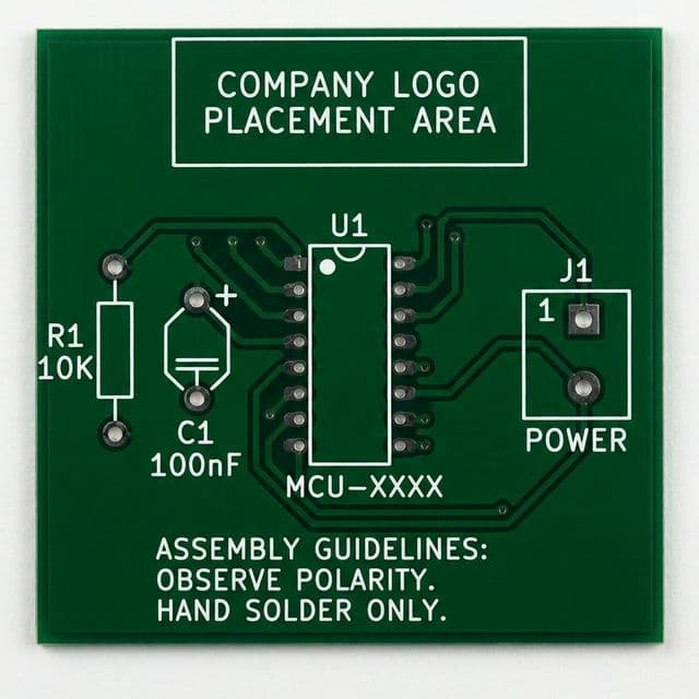
Silkscreen Layer
Component outlines, reference designators, polarity marks, and assembly guidelines for manufacturing.
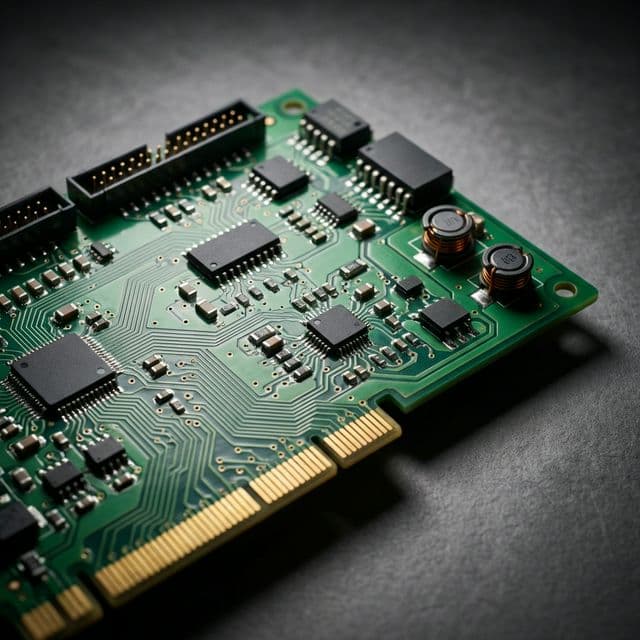
Assembled Board
Photorealistic 3D render of a fully assembled PCB with surface mount components and gold connectors.
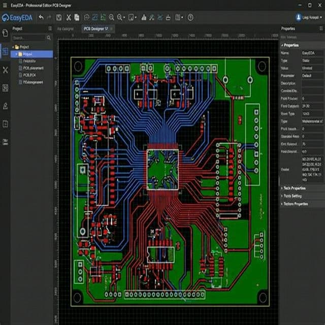
EasyEDA Layout
Complex double-sided PCB routing in EasyEDA with front (red) and back (blue) copper layers, component placement optimization.
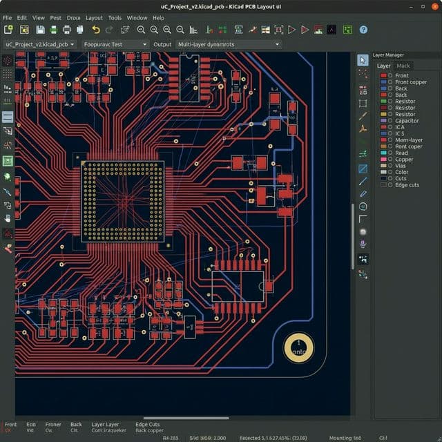
KiCad Multi-Layer Design
Microcontroller-based circuit board layout in KiCad with advanced routing, BGA fanout, and multi-layer stackup.
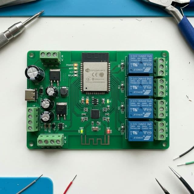
ESP32 Relay Controller
Custom IoT board with ESP32 module, 4-channel relay array, USB-C power, screw terminals, and status LEDs for home automation.
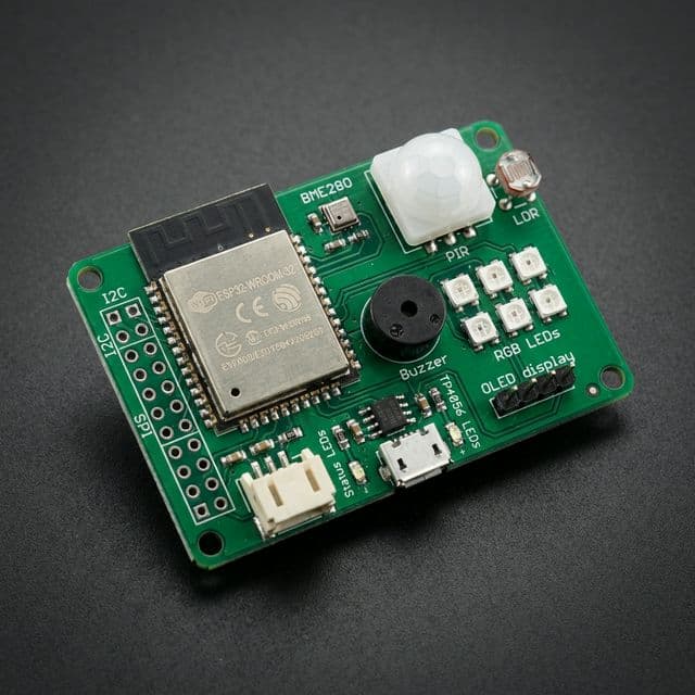
IoT Multi-Sensor Board
Compact sensor hub featuring ESP32, BME280, PIR motion sensor, LDR, buzzer, RGB LED array, OLED connector, and battery charging circuit.
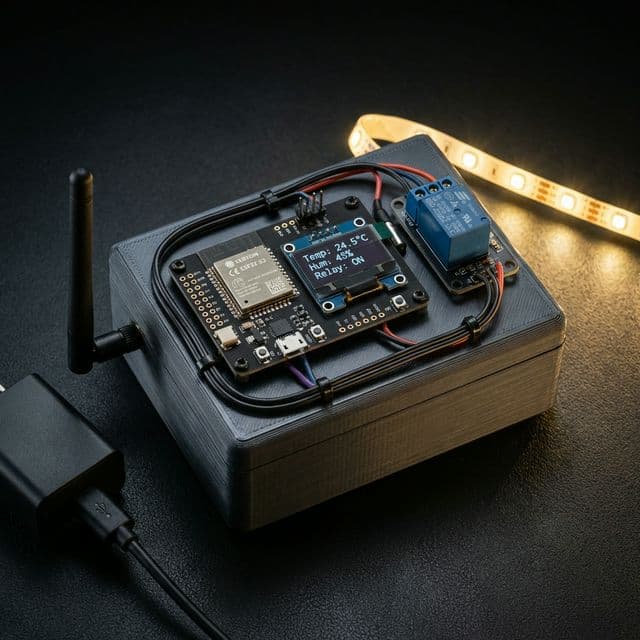
Complete IoT System
Fully assembled IoT project with ESP32, OLED display showing live sensor data, relay module, LED strip control, all in a 3D-printed enclosure.